返回
返回
功率因数校正电路环路稳定性新技术
2017-05-11
This paper describes how to test the feedback loops in power factor correction (PFC) chips for stability. It discusses measurement techniques, stability guidelines, and loop bandwidth considerations for a range of manufacturers and integrated circuits (ICs), with emphasis on the new ICs developed recently. Stability testing is important because loop bandwidth and stability affect how fast the circuit will respond to source voltage transients and load changes. Power factor correction circuits often have two feedback loops. Both loops can have stability problems, and both loops can be tested for stability. One is a relatively slow loop that senses and sets the average output voltage. The other is a relatively fast loop that senses the instantaneous AC input voltage and tries to make the AC input current proportional to it. This second loop has a dynamically changing operating point and presents special measurement challenges. This paper describes procedures for testing both loops and gives guidelines and examples for …several chips.
本文介绍了如何测试功率因数校正(PFC)芯片的反馈回路的稳定性。讨论了测量技术,稳定性准则,以及一系列的厂家的环路带宽的考虑和集成电路(IC),最近在新的IC开发重点。稳定性测试是很重要的因为环路带宽和稳定性影响如何快速的响应电路源的瞬态电压和负载的变化。功率因数校正电路通常有两个反馈回路。两个循环可以有稳定的问题,和两个循环可以测试稳定性。一个是一个相对缓慢的循环,感应且设置平均输出电压。另一个是相对快速循环,感应的瞬时输入交流电压和试图使交流输入电流成正比。这第二次回路具有动态变化的工作点,并提出了特殊的测量挑战。本文介绍了用于测试循环程序和提供指南和例子给……几个芯片。
Introduction
介绍
Power factor correction is being increasingly required as a feature of new power supply designs. Power factor correction takes the form of a new "front end" of power supplies, adding circuitry to shape the input current into an image of the input voltage and therefore making the power supply input look resistive to the source, usually the AC mains. One power supply vendor told us recently "every new specification I receive requires power factor correction, even at power levels as low as 200 watts."
功率因数校正越来越需要新的电源特征设计。功率因数校正采取了一个新的“前端”的电力供应形式,增加电路来塑型输入电流成为输入电压的图像,因此使电源输入对于源看起来是电阻性的,通常是对于交流电源。一个电源供应商最近告诉我们“我们最近收到的每一个新的规范都要求功率因数校正,甚至是在低于200W的功率水平”。
The impetus for this requirement is new regulations, both in the U.S.A. and Europe, limiting the harmonic content of the input current of electrical equipment. This requirement has good and bad side effects. The good, of course, is that electrical power waveforms around the world will be cleaned up considerably when enough time has passed for these new units to supplant older designs now in the field. The bad is that the efficiency of power supplies is reduced, due to the double conversion required, and the size, weight, complexity, and cost of new designs inevitablywill increase to accommodate the new feature.
这种需求的动力是新的规定,无论是在美国还是欧洲,以限制电气设备的输入电流的谐波含量。这种要求有好的也有坏的副作用。对于好的,当然,世界上的电源纹波将在足够的时间内旧设备被新设备所替代后而大规模清理掉。坏的情况是,由于需要双转换,这降低了电源的效率,而且尺寸重量和新设计的复杂性,不可避免地会增加成本以适应新的特性。
In addition to the new circuitry, one or two additional feedback loops are required to control at least the output voltage of the new circuitry, and usually the input current waveform as well. The bandwidth of the voltage loop is critical since if it is too slow the system will not have a timely response to transients, and if too fast, it will distort the input current waveform and destroy the very reason the circuitry was added in the first place. The current loop, if there is one, also has critical bandwidth and stability criteria and moreover is very difficult to measure since the operating point of the circuit is constantly changing as the line voltage changes. Venable Industries is a company dedicated to testing and optimizing feedback loops, hence our interest in this subject.
除了新的电路,至少一个或者两个额外的反馈回路需要来控制新电路的输出电压,而且通常还有输入电流的波形。电压环的带宽很重要,因为如果它太慢,系统将不会有顺便的及时响应,如果太快,它又会扭曲输入电流波形这就破坏了新电路加入进来的首要原因。对于电流环,如果可有,也有关键带宽和稳定性判据而且是非常难以衡量的,因为电路工作点是随着线电压变化而不断变化。Venable公司一直致力于测试和优化反馈回路,所以我们对此非常感兴趣。
Overview
综述
There are four, or perhaps five, approaches to implementation of power factor correction circuits. These are:
Discontinuous Flyback (constant frequency) Continuous Boost-average current sensing (usually constant frequency)
Continuous Boost-peak current sensing (usually constant frequency)
Boost-peak current sensing with current reset to zero each cycle (variable frequency)
Continuous Boost-hysteretic current sensing (variable frequency). This is a special chip made only by Cherry Semiconductor that controls both the peak and valley of the inductor current.
这里有四个或者五个对于功率因数校正电路的实现方法。
不连续的反激式(固定频率)连续平均BOOST电流传感(通常是恒定频率)
连续的BOOST-peak电流传感 (恒频率)
每个周期电流归零的BOOST-peak电流传感 (变频)
连续的Boost-hysteretic电流传感 (变频),这是Cherry Semiconductor专用芯片
Discontinuous Flyback
不连续反激式
The discontinuous flyback, shown in Figure 1, is the simplest of all the PFC circuits. It operates on the principle that discontinuous flyback converters, operated at fixed duty cycle and fixed frequency, draw current from the line directly proportional to the input voltage with no feedback or other special measures required to make this happen. In this special case there is only one feedback loop, the one to regulate output voltage. This is done by sensing the output voltage, comparing it to a reference in an op amp, and using the op amp output to control the duty cycle of the pulse width modulator (PWM). The disadvantages of this approach are that the peak current and voltage on the power transistor are much higher than with other approaches and that considerable filtering is required to smooth the current pulses into a sine wave.
对于不连续反激式,如图1所示,是简单的PFC电路。它运行遵循不连续反激转换器的原理,操作在固定的周期和固定的频率,从线路中直接引来与输入电压成比例的电流而不包含反馈或者其他特殊的要求措施。在这种特殊的情况下,只有一个反馈回路来调节输出电压。这是通过检测输出电压,比较它和一个运算放大器的参考,并使用运算放大器的输出控制脉冲宽度调制(PWM)的占空比。这种方法的缺点是,功率晶体管峰值电流和电压远高于其他方法,相当多的过滤要求平滑脉冲电流为正弦波。
Continuous Boost with Average Current Sensing
通过平均电流感应的持续BOOST电路
Most PFC circuits use the boost converter topology. Figure 2 shows a boost converter with average current sensing. The current sense resistor is placed in the DC return leg opposite the energy storage inductor. The advantages of this boost topology are that the input is a relatively smooth waveform and therefore easy to filter, and that there is a convenient place to sense current (as shown) so that the current can be controlled to match the input voltage waveform. This approach (and all the other boost converters) has two feedback loops. One is a fast loop that controls the instantaneous input current to have the same shape as (make it proportional to) the instantaneous input voltage. The other loop is a slow loop that adjusts the overall amplitude of the input current (and therefore the output current) to keep the output voltage constant. As before, the performance of each of these loops is critical to achieving the goal of low power factor. Fortunately, most loops can be tested in a straightforward manner using standard Venable techniques.
大多数PFC电流使用BOOST变换器的拓扑结构。图2就显示了一个平均电流感应的boost变换器。电流感应电阻放置在相对于储能电感的DC返回引脚。该升压拓扑结构的优点是,输入的是一个比较平滑的波形,因此很容易过滤,并且有一个感应电流方便的地方(如图所示),电流可以控制与输入电压波形。这种方法(而且所有其他的boost变换器)具有两个反馈回路,一个是一个快速环路控制瞬时输入电流具有相同的形状作为(使它成正比)的瞬时输入电压。另外是一个缓慢的循环,调节输入电流的振幅(因此输出电流)保持输出电压恒定的。像以前一样,每一个回路的性能是实现功率因数低的目标的关键。幸运的是,大多数循环可以使用标准化VENABLE技术来进行简单的测试。
This particular implementation, average current sensing, should give the best overall performance if implemented correctly because the variable being sensed (instantaneous input current) is exactly the one that needs to be controlled. The difficulty comes from the fact that the instantaneous input voltage is a rectified sine wave and is changing from zero to the peak value and back to zero 100 or 120 times per second, and this is the reference signal the current has to track. (This difficulty is shared by all boost topologies.)
对于平均电流感应这种特殊的实现,应该给与好的整体性能如果能够完全的正确实施。因为被测变量(瞬时输入电流)是一个需要被控制的量。困难来自于实际上的瞬时输入电压整流正弦波每秒内从0到峰值100-120次,这是电流跟踪参考信号(这也是所有boost拓扑结构共有的困难)。
Continuous Boost with Peak Current Sensing
峰值电流感应持续boost电路
A power supply control approach that has become popular in recent years is that of current mode control. In this approach, the peak transistor current is the directly controlled variable rather than duty cycle as in the previous approach. This is not as accurate as the average current approach since the controlled variable (peak current) is not exactly equal to the desired variable (average current), but since the peak-to-peak inductor ripple is relatively small (typically 10% of the DC value) the error introduced is not large and reasonable power factor can be achieved with this approach.
电源控制方法,已成为近年来流行的电流模式控制。在这种方法中,晶体管的电流峰值是直接控制变量而不是在以前方法中的占空比。这与平均电流方法不一样准确,因为控制变量(峰值电流)不完全等于所需的变量(平均电流)。但是因为峰值电感纹波比较小(一般是10%的DC值),引入的误差不大,所以可以用这放大得到合理的功率因数。
Figure 3 shows a boost converter with peak current sensing. The current sense resistor is series with the source of the power FET. Transistor current is initiated by the PWM clock and terminated when the transistor current reaches a peak level proportional to the instantaneous value of input voltage. Since PFC boost converters operate at a duty cycle greater than 50% for at least a portion of the input waveform, slope compensation must be incorporated to prevent open loop oscillation of the current mode control loop. Most current mode PFC ICs have provision for slope compensation.
图3显示了一个升压转换器的峰值电流传感。电流检测电阻和功率FET的源极串联。晶体管电流由PWM时钟启动,当晶体管电流达到输入电压的瞬时值成比例的峰值终止。由于PFC升压转换器工作在一个工作周期大于50%的输入波形的至少一部分,必须纳入防止斜坡补偿的电流模式控制回路的开环振荡。大多数的电流模式的PFC IC有斜坡补偿条款。
As in the other boost topologies, there are two feedback loops. One, the slow loop which controls the constant of proportionality between input voltage and input current, is the same as before with the requirement of a tightly controlled bandwidth to prevent both slow response to transients and distortion of the current waveform. It is essential to measure this bandwidth at least on a sample basis, if not on every production unit. The performance will vary from chip-to-chip and vary significantly from lot-to-lot, especially if chips from more than one manufacturer are used interchangeably.
在其他的boost拓扑结构中,有两个反馈回路。一:慢速回路控制输入电压和输入电流比例常数,与之前要求一样严格控制带宽以防止瞬态反应迟钝和电流波形畸变。它是衡量该带宽的必要条件,如果不是在每一个生产单元而至少在一个简单的样本里。芯片与芯片之间的性能会不同而且特性上会有很大差异,特别是一种芯片在不同的厂商之间交替使用。
The other, the fast current loop which controls input current, presents special measurement problems but is also essential to measure because of the possibility of oscillation due to current mode control operated at greater than 50% duty cycle. It is not possible to measure the open loop gain of the current loop directly because it is essentially digital. It is easy, however, to measure the closed loop gain. The closed loop gain is the transfer function from reference input (usually the output of an internal multiplier) to the input current, which is the energy storage inductor current and can be measured with a current probe on one of the inductor leads. The stability of the open loop gain can inferred from this closed loop measurement. Figures 4 and 5 show typical closed loop transfer functions for circuits with open loop bandwidth of 3.16 kHz and phase margins of 72° and 20° respectively.
另外,快速电流环控制输入电流,提出了特殊的测量问题,但也是必不可少的措施由于电流模式控制在大于50%的占空比操作振荡的可能性。这是不可能直接测量电流环的开环增益,因为它本质上是数字。然而,它是容易的,测量的闭环增益。闭环增益是从参考输入的传递函数(通常是一个内部乘法器的输出)的输入电流,这是储能电感电流可以用电流探头的一个电感引线。的开环增益的稳定性可以从这个闭环测量推断。图4和图5显示了典型的闭环传递函数对电路的开环3.16千赫带宽和相位裕度分别为72°和20°。
There will be more and more peaking in the closed loop transfer function as the phase margin of the open loop transfer function is reduced. Phase margin of current mode control loops is adjusted by the amount of slope compensation provided. The open loop gain can also be calculated from closed loop data with proper software tools.
会有越来越多的闭环传递函数的峰值出现随着开环传递函数的相位裕度降低。电流模式控制回路的相位裕度是由提供的斜坡补偿量进行调整。开环增益也可以从适当的软件工具的闭环数据计算。
Boost with Current Reset to Zero
电流重置到0的boost电路
Another control approach with boost converters looks like current mode control, but incorporates additional circuitry to sense when the inductor current declines to zero in the off portion of the power transistor cycle. At that point the transistor is triggered on again, rather than from a PWM clock as in conventional current mode control. The net result of this arrangement is a waveform that always starts from zero, reaches a peak equal to twice the average for that instant of time, and then declines to zero again. Figure 6 shows a schematic with typical waveforms. The advantages of this approach are:
另一种boost变换器控制方法看起来像是电流模式控制,但是当电感电流下降到0时在晶体管周期部分,采用了额外的电路来感应。在这一点上晶体管再次触发,而不是从一个PWM时钟在传统的电流模式控制。这种安排的最终结果是一个波形总是从0开始,达到一个峰值的时间等于两倍达到平均水平的时间,然后下降,再到0。图6显示了一个典型的波形示意图。这种方法的优点是:
Since the current waveform is a triangle wave with zero current as a base, the controlled variable (peak current) is theoretically exactly twice the average current, so the performance of the power factor control aspect of the circuit should approach that of the average current mode control scheme. Because the current is constrained to a fixed value (zero) at one point in every cycle, one degree of freedom is removed from the state equations and slope compensation is not required to make the circuit openloop stable. The energy storage inductor is relatively small. Transistor turn-on losses are eliminated
由于电流波形是以0电流为基础的三角波,控制变量(峰值电流)在理论上实际上是两倍的平均电流,所以电流功率因数控制方面的性能应该接近平均电流模型方案。因为电流是被限制为一个固定值(0)在每个周期中由一个点,所以使开环电路稳定的话,状态方程的一个自由度和谐波补偿电路是不必要的。储能电感相对较小,晶体管导通损耗被淘汰。
The Disadvantages Are
不利因素
The peak current in the transistor is almost twice that of other boost schemes. Transistor turn-off losses are at least doubled Extra filtering is required to smooth the large AC waveform drawn by this approach.
晶体管的峰值电流几乎是其他boost方案的两倍,晶体管损耗至少翻番,额外的过滤使得要求大型交流波形更为平滑。
As can be seen from the above advantages and disadvantages listing, no one approach is perfect and engineers can rest assured that their judgment will still be needed to select from the many approaches available.
从以上可以利弊清单中看到的,没有一个方法是完美的,工程师们可以放心,他们的判断仍将需要从许多可用的方法中选择。
Boost with Hysteretic Control
滞后控制boost电路
A special case of the above approach is one invented some years ago by Cherry Semiconductor where both the peak and valley of the current waveform are controlled. Cherry calls this Hysteretic Control. This approach also removes a degree of freedom from the circuit and removes the need for slope compensation. Since the difference between the controlled variable (peak current) and the average current is known and programmable, accurate power factor control is also achievable. The AC ripple on the inductor can also be controlled, usually to the same general range (10% of DC) that the other boost PFC circuits use.
上述方法的一个特例是一些年前由Cherry半导体公司的一个发明,电流波形的峰谷的控制。Cherry称这种为滞环控制。这种方法还消除了程度的自由和消除斜坡补偿电路的需要。由于控制变量之间的差异(峰值电流),平均电流是已知的,可编程的,精确的功率因数控制也是可以实现的。对电感的交流纹波也可以控制,通常以相同的一般范围(10%直流),其它的Boost PFC电路的应用。
List of Available Integrated Circuits
可用集成电路清单
Table 1 above shows a reasonably comprehensive list of power factor correction integrated circuit manufacturers, the chips they make, and the characteristics of these chips. Each manufacturer differentiates itself by supplying a different set of features, simplifying either the chip design or the external circuitry. Please refer to individual data sheets that are available from the various manufacturers for specifics on the particular combination of features and benefits of a particular chip.
上面的表1显示了一个合理的综合的功率因数校正集成电路生产企业名单,他们制作的芯片和这些芯片的特点。每个制造商通过产品一些不同的设置来区分,简化的芯片设计或外部电路。请从对特定芯片的特点和优势,结合特定的细节和个人数据来采用所需要的芯片。
Typical Block Diagrams of Average and Peak Boost PFC
平均和峰值boost PFC典型框图
Figures 7 and 8 are simplified block diagrams of the two principal boost converter topologies. They show the signal flows clearly. Average current control (similar to voltage mode control) has an extra operational amplifier to control the current. Peak current control (similar to current mode control) compares the peak switch current to a rectified sine-wave reference signal and terminates the switch current when it equals the reference.
图7和图8是两种主要的Boost变换器拓扑结构的简化框图。他们清晰地显示了信号流。平均电流控制(类似于电压模式控制)来控制电流的一个额外的运算放大器。峰值电流控制(类似于电流模式控制)比较了峰值开关电流,对于一个整流正弦参考信号,当它等于参考时,终止开关电流。
Average current boost PFC
平均电流boost PFC
Figure 7 shows a typical average current boost power factor correction circuit.
图7显示了一个典型的平均电流boost功率因数校正电路。.jpg)
The input AC waveform is rectified to produce a half-sine-wave voltage with a peak value of about 160 volts on 120-volt mains or 320 volts on 240-volt mains. There is very little capacitive filtering directly across the rectified line input. Any current, which flows from the input, flows through the energy storage inductor and returns through the current sense resistor. When the power FET turns on, energy is stored in the inductor, and when the power FET turns off, at least some of this energy is delivered to the output filter capacitor and load (not shown) through the diode. With boost converters, the output voltage must be higher than the maximum input voltage. Typical output voltage is 380 to 400 volts DC This output voltage is divided down and compared to a reference in the voltage error amplifier. This is the slow loop, and it needs to have a bandwidth in the range of 10 to 12 Hz. The output of this error amplifier is fed to one input of a multiplier and is used to scale the value of the other input of the multiplier, which is a current proportional to the half-sine-wave rectified input voltage.
输入交流波形整流产生一个正弦半波电压,120V的线路中峰值为160V或者240V线路中峰值为320V。有非常小的电容滤波直接在整流线路输入。任何电流,来自于输入端,流过储能电感和返回通过电流检测电阻。当功率场效应晶体管打开,能量储存在电感,当功率场效应管关闭,至少有一些能量传递到输出滤波电容和负载(未显示)通过二极管。升压转换器,输出电压必须高于最高输入电压。典型的输出电压为380到400伏直流。输出电压分下降相比参考一个电压误差放大器。这是慢回路,它需要在一个带宽10到12赫兹的范围内。该误差放大器的输出馈送到事半功倍的一个输入,用于规模乘法器的输入值,这是成比例的电流的正弦半波整流的输入电压。
The output of the multiplier is a signal (usually a current) with a half-sine-wave rectified shape and amplitude proportional to the output of the voltage error amplifier. This signal is compared to the input current by summing the multiplier output with a current proportional to input current at the positive input of the current error amplifier. The other (negative) input of the current error amplifier is grounded through a resistor, and the current feedback loop acts to keep the positive input at ground potential (zero volts). The output of the current error amplifier is compared to a ramp and used to generate a pulse-width-modulated drive signal for the power FET.
该乘法器的输出是一个半正弦波整流塑型信号而且幅值与电压误差放大器的输出成比例。这个信号是相对于输入电流通过乘法器的输出与输入电流成比例的电流在电流误差放大器的正输入。另一个(负)电流误差放大器输入通过电阻接地,而且电流反馈回路表现保持正的输入对地电压(0V)。电流误差放大器的输出相比于一个斜面而且被使用来产生一个用于场效应管的脉冲宽度调制信号。
Peak Current Boost PFC
峰值电流boost PFC
Figure 8 shows a typical peak (current mode) power factor correction circuit. As before, the input from the AC mains is rectified to produce a half-sine-wave rectified voltage that varies from zero to about 360 volts, depending on the AC mains voltage. With peak current boost PFC, the average current is not important and the current sense resistor is typically placed in series with the source terminal of the power FET. As before, the output voltage must be greater than the maximum input voltage, and is typically 380 to 400 volts DC This voltage is sensed with a divider string and compared to a reference in the voltage error amplifier. As before, this is the slow loop and should have a bandwidth between 10 and 12 Hz. Like the average current circuit, the half-sine-wave rectified AC input voltage is fed to one input of a multiplier and the voltage error amplifier output is fed to the other, so that the multiplier output is again a half-sine-wave rectified waveform scaled in amplitude by the output of the voltage error amplifier.
图8显示了一个典型的峰值(电流模式)的功率因数校正电路。像以前一样,交流电源的输入整流产生一个从0到360V变化的正弦半波整流电压,根据不同的交流电源电压。峰值电流boostPFC,平均电流是不重要的,而且电流检测电阻通常是放置在与功率FET所串联的电源终端上。像以前一样,输出电压必须大于最大的输入电压,通常是380-400V的直流电压检测带分隔字符串比较参考电压误差放大器。之前,这是慢回路和应具备10-12HZ之间的带宽。比如平均电流电路,正弦半波整流交流输入电压馈送到一个乘法器的输入而且电压误差放大器输出亏送到另外一个输入,所以通过电压误差放大器输出乘法器输出也是一个去鳞的正弦半波整流波形。
At this point, operation of the two circuits differs. The power FET current is compared to the halfsine-wave rectified reference signal, and when it equals this signal the power FET is turned off.
在这一点上,两个不同的电路的操作。功率FET电流相对于矩形波整流的参考信号,当它等于该信号的功率场效应晶体管是关闭的。
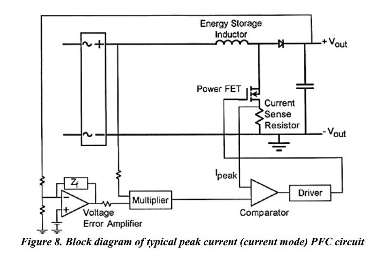
The power FET remains off until it is turned on again by a fixed-frequency clock, which is part of the PFC control chip. A compensating ramp usually derived from the clock oscillator (ramp and clock not shown in the diagram) is either subtracted from the reference signal or added to the current signal to provide open loop stability of the current mode control circuit when the duty cycle exceeds 50% as it does at low input voltage. This type of regulation, current mode control, does not lend itself to testing. The best way to test for stability of the current loop is to inject a current in parallel with the multiplier output and then to measure the transconductance from control voltage (output of the multiplier) to controlled output (current in the energy storage inductor). In order to do this, the operating point must be frozen (as explained later in this paper), and the test results compared to plots like those given in Figures 4 and 5 earlier in this paper.
功率场效应管保持关闭,直到它被打开了一个固定频率的时钟,它是PFC控制芯片的一部分。一个补偿斜坡通常来自时钟振荡器(斜坡和时钟不在图中所示)是减去参考信号或添加到电流信号提供的电流模式控制电路的开环稳定性当占空比超过50%是在低输入电压。这种类型的调节,电流控制模式,不适合测试。对电流环的稳定性测试的好的方法是将并行乘法器的输出电流,然后测量从控制电压的跨导(乘法器的输出)来控制输出(在储能电感电流)。为了做到这一点,操作点必须冷冻(正如在本文后),本文前面给出的图4和 图5实验结果的比较。
Specific Examples of Average and Peak PFC Circuits
平均和峰值PFC电路的具体实例
Figures 9 and 12 are specific examples of average and peak power factor correction circuits. There are variations from manufacturer to manufacturer in the specific implementations of the circuits required. There are also differences in features. The two examples chosen demonstrate the many choices that are available from the various vendors.
图9和图12是平均和峰值功率因数校正电路的具体实例。他们是从不同的供应商所供应要求的不同电路需求的实例变化而来,它们也有不同的特点,这两个例子的选择也证明在许多供应商中有着很多不同的选择。
Average Current PFC Circuit, the Linear Technology LT1249
平均电流功率因数校正电路,the Linear Technology LT1249
Figure 9 is a simplified block diagram of the LT1249 power factor correction IC, redrawn from the schematic furnished in the Linear Technology data sheet. The block diagram also shows injection points for feedback loop testing.
图9是一个简化的块的lt1249功率因数校正电路图,从图中绘制提供线性技术数据表。方框图也显示了反馈回路测试的注入点。
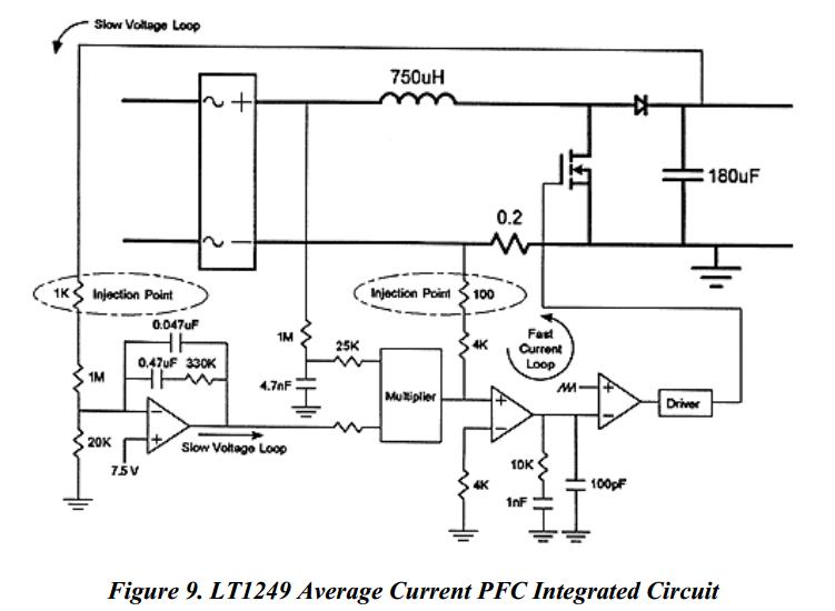
The voltage control loop, "slow voltage loop" in this example, senses the output voltage with a resistive divider and compares the result to a 7.5-volt reference. The nominal output voltage in this case will be 382.5 volts. Provision is made for a zero and pole in the amplifier transfer function to adjust the loop phase margin. The ideal bandwidth for this loop is 10 to 12 Hz, and the phase margin should be between 50 and 70 degrees. The problem for the designer, which he or she will probably pass on to the user, is that the actual loop performance depends on the multiplier parameters and these are not specified in the data sheet. For this particular part, only a typical value of multiplier output current is given, with no min or max value. That is why it is essential to test the feedback loop, at least on a sample basis if not on every production unit. If you are a purchaser or user of power supplies with PFC incorporated in the design, ask for data on the loops periodically (not just on the qualification unit). This data should come in the form of a Bode plot, which is a plot of gain and phase versus frequency, clearly showing the bandwidth and phase margin.
电压控制回路,“慢电压回路”在这个例子中,输出电压的感测电阻分压器和比较的结果参考7.5V。标称输出电压在这个案例中为382.5V。设置规定在放大器传递函数的零点和极点来挑战环路相角裕度。理想的环路带宽是10-12HZ,相角裕度在50到70°之间。对于设计师的问题,他们可能会通过用户得知,这是目前乘法器没有指定的数据表。对于这个特殊的部分,只有典型的乘法器的输出电流值给出了在最小或者最大值的公式。这就是为什么它是必要的反馈回路试验样品的必需,就算不是每个产品单元也至少在一个样本中。如果你是买方或者PFC研究与设计公司电源的使用者,间歇性的询问在环数据(不只是定期)这种数据可能是伯德图的形式,一个相位随着频率变化的增益图,可以清晰显示带宽与相角裕度。
Operation and Testing of the Current Feedback Loop (fast loop)
电流反馈回路的操作与测试
The other feedback loop in the LT1249 is the fast loop that senses the input current and controls it to make it match the shape of the input voltage. This loop should have a bandwidth of at least 3 kHz, again with phase margin of 50 to 70 degrees. This loop must be tested also since the loop gain is dependent on the transconductance of the internal error amplifier and the transconductance varies almost 4:1 according to the data sheet. The reference for this loop is the multiplier output current, which has the shape of a rectified sine wave and an amplitude controlled by the output of the voltage error amplifier (slow loop). Current flowing through the 0.2-ohm current sense resistor creates a voltage, which causes current to flow upward in the 4K input resistor to the fast current loop error amplifier. In this case, the reference current from the multiplier and the current from the controlled variable (input current) through the 4K resistor sum at the positive input of the current error amplifier. The negative input of the error amplifier is grounded through another 4K resistor, so any difference from zero volts at the positive input is amplified and forms a reference voltage for the PWM comparator. A fixed amplitude, fixed-frequency ramp is applied to the other input of the comparator, and the points where the ramp crosses the DC level from the error amplifier output set the switching points and thereby duty cycle of the power FET.
在lt1249其他反馈回路的快速循环,感官的输入电流和控制它,使它与输入电压的形状。这个循环应该有一个至少3 kHz的带宽,再以50至70度的相位裕度。这个循环必须进行测试,同时由于环路增益依赖于内部误差放大器的跨导和跨导变化几乎4:1根据数据表。这个循环的参考是乘法器的输出电流,它的形状是一个整流正弦波和振幅控制的输出电压误差放大器(慢回路)。流经0.2-ohm电流检测电阻产生电压电流,使电流上升在4K的输入电阻的快速电流回路误差放大器。在这种情况下,从乘法器和电流控制变量的参考电流(输入电流)通过4K的电阻和在电流误差放大器的正输入。误差放大器的负输入是通过另一个4K的电阻接地,所以任何差异从零伏的正输入放大,形成PWM比较器的参考电压。一个固定的放大器,固定频率斜坡应用于比较器的另一输入,和点斜穿过直流电平的误差放大器输出设置开关点和功率FET周期。
The problem with this fast current loop is that the dynamic operating point is constantly changing. When a frequency response analyzer is used to measure loop gain in a conventional way, the resulting Bode plot is actually an average of all the Bode plots from very low current to the peak current. The loop can and sometimes does oscillate either at very low or very high current, while showing stability on an average basis.
这种快速电流环路的问题是动态工作点是不断变化的。当频率响应分析仪用传统方式去测量环路增益时,得到的伯德图实际上是一个所有伯德图的平均值,从非常低的电流到峰值电流。环路可以而且有时会在非常低或者非常高的电流时振荡,而呈现出在平均基础上的稳定性。
The solution to this problem is to "freeze" the operating point of the current loop. This "freezing" requires setting DC values for the input and output voltages and for the output of the voltage error amplifier so that the operating point of the circuit represents actual conditions for some instantaneous point of time. The instantaneous input voltage is given by
解决这个问题的办法是“冻结”的电流环的工作点。这种“冻结”需要设置直流值为输入和输出电压和电压误差放大器的输出,该电路的工作点,代表了一些时间瞬时点的实际情况。瞬时输入电压是:
Ein = Vrms * sqrt(2) * sin(theta)
where Ein is the test DC input voltage, Vrms is the rms value of input voltage if AC voltage were being used in the test, and is the equivalent input sine wave phase angle for the operating point being tested. The instantaneous input current Iin for a given input power level Pin is given by the equation
Ein是测试直流输入电压,Vrms是输入电压的rms值,如果是交流电压用于测试。等效输入正弦波操作点的相角也会被测试。瞬时输入电流lin在一个给定的输入功率电平引脚是由下式给出
Iin = (Pin / Vrms) * sqrt(2) * sin(theta)
where Iin is the DC input current and the other terms are as previously defined. The output voltage is set by connecting the output of the PFC circuit to an adjustable shunt regulator. The final step in "freezing" the operating point is to disable the voltage error amplifier (typically by shorting the negative input to ground) and then using a DC power supply with a resistive load if necessary to supply the voltage normally supplied by the error amplifier output. This voltage is used to set the DC input current Iin to the value calculated in the previous equation. Figure 10 shows the simplified block diagram with these changes implemented so the current loop can be tested.
这里lin是直流输入电流,其他条款如先前定义。输出电压由PFC电路的输出连接到一个可调并联稳压器。最后一步,在“冻结”的工作点是禁用的电压误差放大器(通常通过做空负输入地),然后用直流电源与负载电阻如果必要的供应通常由误差放大器输出电压。这个电压是用来设置直流输入电流IIN在以前的方程的计算值。图10显示了简化框图与这些变化实现电流环可以测试。
The technique for testing the stability, bandwidth, phase margin, and gain margin is given in detail in reference 2, but a simplified version is as follows:
这个技术用于测试稳定性,带宽,相角裕度,增益裕度,见参考文献2,但是给了一个简化的版本如下:
Figure 11 is a block diagram of a test setup for making loop measurements. Care has to be taken in choosing test equipment since the voltages involved are near 400 volts. For the voltage loop, the injection transformer is connected across the 1K resistor in series with the 1M resistor and the frequency is swept from at least 1 Hz to 100 Hz. The voltage on each side of the injection resistor is measured and recorded at each measurement frequency, and the ratio of output voltage (across the 180 µF capacitor) to the input voltage (voltage at the junction of the 1K injection resistor and the 1M resistor) is plotted versus frequency to form a Bode plot. The bandwidth is the frequency at which the gain is unity (zero dB), the phase margin is the phase reading when the gain is unity and the gain margin is gain (in dB) when the phase reading is zero. The goal is 10 to 12 Hz bandwidth with 50 to 70 degrees of phase margin.
图11是一个使回路测量测试装置框图。应当注意测试设备的选择因为涉及的电压是400伏特附近。对于电压回路,注入变压器连接在1K的电阻与1m电阻和频率系列是从至少1赫兹到100赫兹扫描。对每侧的注射电阻电压测量和记录在每个测量点的频率,以及输出电压的比值(在180µF电容器)的输入电压(电压在1K电阻器的接线和注射1m电阻)作图频率形成的Bode图。带宽是频率的增益是统一的(零分贝),相位裕度为相的阅读时,增益和增益裕度统一增益(dB)当相位读数为零。目标是10到12赫兹的带宽与50到70度的相位裕度。
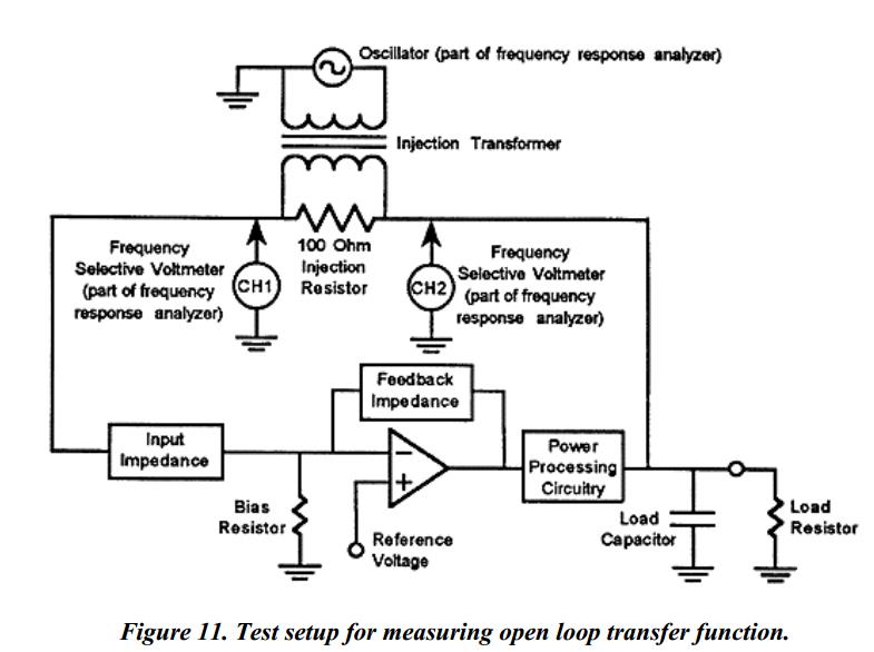
The current loop is measured by first "freezing" the operating point as described earlier, then connecting the injection transformer across the 100 ohm injection resistor in series with the 4K input resistor to the error amplifier of the fast current loop. As before, the loop gain is measured as the ratio of the output (junction of the 100 ohm injection resistor and the 0.2 ohm current sense resistor) to the input (junction of the 100 ohm injection resistor and the 4K input resistor). This loop needs to be fast, with a bandwidth of at least 3 kHz, since the reference is quickly changing and the controlled output (input current) must track this reference signal with minimal phase delay. As usual, 50 to 70 degrees of phase margin is an ideal tradeoff between maximizing response time and minimizing overshoot and ringing. Measurement should be made at several operating points.
电流环是由第一个“冻结”的工作点,如前所述测量,然后穿过100欧姆的串联在4K输入电阻的电阻上连接注入变压器到快速电流环的误差放大器。之前,环路增益测量的输出比率(100欧姆的电阻和注射0.2欧姆电流检测电阻连接)的输入(100欧姆的电阻连接和注射4K的输入电阻)。这个循环需要快速,用一个带宽至少为3千赫,由于参考正在迅速改变和控制输出(输入电流)必须以最小的相位延迟跟踪该参考信号。像往常一样,50到70度的相位裕度是的最大响应时间和尽量减少过冲和振铃的理想的权衡。测量应在多个操作点。
Peak Current PFC Circuit, the Micro Linear ML4812
峰值电流PFC电路,微型线性ML4812
Figure 12 shows a simplified block diagram of the Micro Linear ML4812 power factor correction circuit with signal injection points and techniques shown also. The current regulation portion of this chip operates in current mode. As with the other chip, the output voltage is divided down, compared to a reference in an error amplifier, and the output of this error amplifier is used in a multiplier to scale the half-sine-wave rectified signal from the input voltage. The output of the multiplier is a half-sine-wave rectified signal, which is applied to one input of a comparator. The other input of the comparator is a voltage proportional to the instantaneous current in the power FET.
图12显示了一个简化的微线性ml4812功率因数校正电路的方框图,信号注入点和技术也显示其中。该芯片的电流调节部分工作在电流模式。与其他芯片相同,输出电压是分压的,与误差放大器的参考相比较,这一误差放大器的输出是用于乘法器的输入电压规模的正弦半波整流信号。该乘法器的输出是正弦半波整流信号,并将其应用于比较器的一个输入。比较器的另一与输入电压成比例的功率场效应管的瞬时电流。
The comparator output controls the power FET, turning it off when the peak current reaches the reference level. The power FET is turned on again by a fixed-frequency clock in the chip. As with all current mode circuits operated above 50% duty cycle, a compensating ramp is required to make the digital current loop stable, and provision for this ramp is provided in the chip.
比较器输出控制功率场效应管,当峰值电流接近参考水平时将其关闭。功率场效应晶体管是打开了芯片中的一个固定频率的时钟。如同所有的电流模式电路操作超过50%的占空比,需要一个补偿斜坡使数字电流环稳定,这个坡道在芯片中提供。
The voltage loop is tested exactly like it is in the average current chip described above. In this case, the injection resistor is in series with a 360K resistor connected to the 380-volt output. The requirements for this voltage loop are the same, 10 to 12 Hz bandwidth and 50 to 70 degrees of phase margin.
电压回路测试完全一样,它是在平均电流上述芯片。在这种情况下,注入电阻与一个连接到380伏输出与360K电阻串联。这个电压回路的要求是相同的,10到12赫兹的带宽和50到70度的相位裕度。
The current loop cannot be tested directly. It can be easily tested indirectly, however. Instead of creating a sinusoidal error voltage in series with the feedback loop as was done in all the previous measurements, a parallel injection scheme is used to disturb the operating point of the loop. The transfer function is then measured from the signal injection point to the controlled variable, in this case, input current. The measurement that results is the closed loop transfer function, the transfer function from reference to output. As before, the operating point has to be "frozen" in exactly the same way in order to do a meaningful measure of current loop stability. Rather than a direct measurement of bandwidth and phase margin, the closed loop transfer function is flat out to about the bandwidth of the open loop transfer function, then starts to roll off. The amount of peaking at the frequency where the roll off starts is related to the phase margin of the feedback loop. By making the closed loop measurements and comparing the results to the sample plots shown in Section 2, accurate assessment of the stability margins can be made. Closed loop data can also be converted to open loop data to see the actual open loop Bode plots. The alternative, described to us recently by a leading power supply manufacturer, is "to follow the circuits in the manufacturer's data sheets and pray a lot."
电流回路不能直接测试,但是可以很简单的间接测试。不同于建立一个正弦误差电压串联在反馈回路中作为之前的测量,一个并联的注入方案被采用来干扰环路的工作点。所测传递函数来源于信号注入点的控制变量,在种情况下,是输入电流。测量结果显示为闭环传递函数,传递函数是来自输出的参考。之前,工作点被“冻结”完全一样是为了做一个有意义的电流环稳定性测量。不是直接的带宽和相角裕度测量,而是与闭环传递函数紧密相关的开环传递函数带宽,then starts to roll off。通过闭环测量和比较第二章简单图像的结果,可以做精确的稳定裕度评估。闭环数据也可以转变为实际的伯德图看到的开环数据。可以选择的是,这些电源生产厂家最近给我们展示的产品都是“遵循制造商的数据表的电路and pray a lot."
2017-02-11